The LP4033 is a fully integrated switch mode charger solution with power path management targeting singlecell Li-ion battery powered portable applications. A low on-resistance BUS-FET is integrated to manage the input power from the VIN pin. A bidirectional buck or boost converter is integrated to manage charging and discharging of the battery. The buck charger supports up to 3-A charging current with up to 95% efficiency. The ultra-low quiescent current boost converter consumes less than 2-μA and supports up to 1.5-A output current. Two independent load switches provide power from the PMID pin to the LDSW1 pin and LDSW2 pin with high accuracy current limit. An NTC circuit is offered to manage the temperature range that charging or discharging is allowed. A LDO pin delivers power to the system that contains an MCU typically. The LP4033 offers power path management that allows the system to be powered up with a fully-discharged battery. It can dynamically manage the power from the VIN input and the battery to meet the system loading needs. An I2C interface enables programming various parameters ofcharging, discharging, and multiple protection functions. An interrupt output (IRQb) sends a signal to the MCU when an interrupt event happens so the MCU can take actions accordingly. Multiple features are offered for the safe operation of the system, including input voltage OVP (over voltage protection), UVLO (under voltage lockout), OTP (over temperature protection), SCP (short circuit protection), etc.When powered by a battery, LP4033 can operate with only 5-µA current. The whole System is in a 24-pin 4 X 4 QFN package.
I2C, 1.5A BOOST,High Vin voltage,3A Large current,OTP,OCP,UVLO
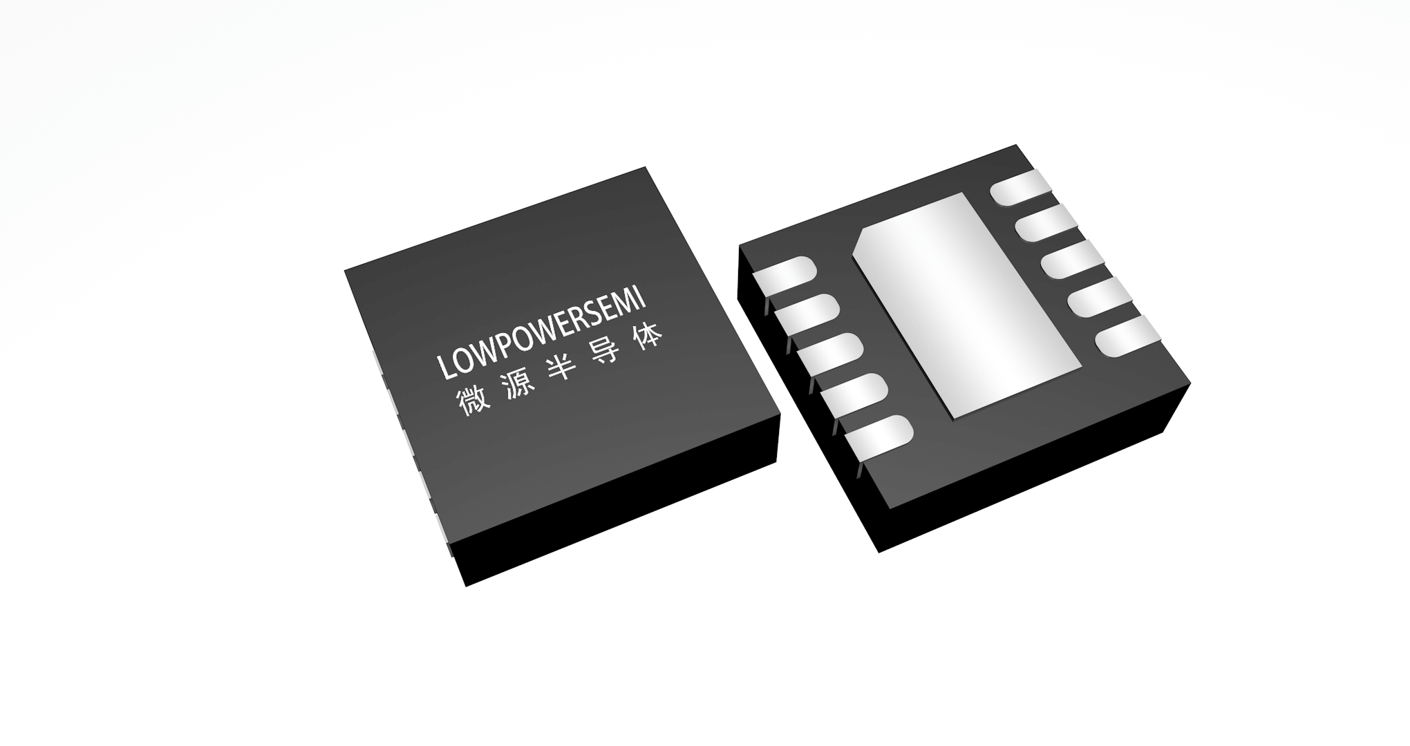
封装
QFN-24(4*4)
特征
特征
◆ Input over-voltage protected up to 30V ◆ Charge management - Programmable charge current up to 3-A with up to 95% switching efficiency - Programmable floating voltage with 0.35% accuracy - Programmable trickle charge and termination current with minimum 30-mA termination current ◆ Automatic re-charge and thermal foldback ◆ I2C bus to the MCU with an interrupt pin ◆ Power path management ◆ Boost converter with up to 1.5-A output ◆ Two independent load switches with up to 600-mA output for each channel ◆ Load insertion and removal detection ◆ Ultra-low quiescent current linear regulator ◆ NTC management ◆ Rich protections: UVLO, OVP, SCP ◆ Minimum 5-µA ultra-low iq in normal operation ◆ 4mm Χ 4mm QFN-24 package ◆ RoHS Compliant and 100% Lead (Pb) Free